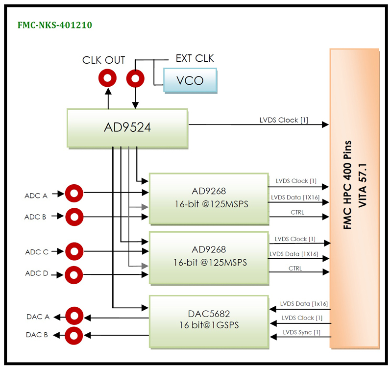
March 19, 2024
 

Slide 1 Slide 1 Slide 1 Slide 1 Slide 1 Slide 1 Slide 1 Slide 1
Search
Technology/Function
Form Factor
Interface
IP Core
FMC-NKS-401210
High Pin Count FMC Module
4- Channel 16-bit ADC 125MSPS
2- Channel 16-bit DAC 1GSPS
 
 
Description

The FMC-NKS-401210 is a four-channel 16-bit ADC at 125MSPS synchronous and maximum sampling rate and dual channel 16-bit DAC at 1GSPS synchronous and maximum sampling rate. This module was designed based on dual-channel AD9268 ADC of Analog Device Company with DDR LVDS or CMOS outputs and dual-channel DAC5682 DAC of TI Company with DDR LVDS inputs. Because of containing a FMC-HPC connector, FMC-NKS-401210 is mechanically and electrically compliant to VITA 57.1 standard. Controlling of clock source, sampling frequency and calibration by a SPI BUS are its other features. The sample clock can be supplied from PLL clock generator, externally through a coax connection or supplied by an internal clock source (VCO). This module can use on every carrier card which follows the VITA 57.1 standards; therefore it can have the maximum data throughput and minimum latency.


Features

ADC's:
• 4 Channels, 16-bit Resolution, 125 MSPS
• Differential Analog Input with 650MHz Bandwidth
• 1.8V CMOS or LVDS Output Signal
• SNR > 75 dBFS @ 20 MHz and 125 MSPS
• SFDR > 85 dBc @ 20 MHz and 125 MSPS
• ENOB > 12.5 Bits @ 20 MHz and 125 MSPS
• Flexible Analog Input Range: 1V p-p to 2V p-p
• Xtalk Isolation > 95dB
• High Performance AC-Coupled Analog Input
• Serial Port Control
• Low Power: 750 mW @ 125 MSPS
• Pin Compatible with AD9650


DAC's:
• 2 Channels, 16-Bit, 1GSPS Update Rate
• 16-Bit Input LVDS Data Bus
• Analog Output with 500MHz Bandwidth
• Phase Noise > 100dBc @ 1kHz and 1GSPS
• Serial Port Control
• 2x-32x Clock Multiplying PLL/VCO
• 2x or 4x Interpolation Filters
• High Performance AC-Coupled Analog Output


Other:
• VITA 57.1 Compliant
• FMC Interface Connector for Digital Output, Power LEDs and Single-ended SMC or other Connectors for AIN, AOUT& EXTCLK
• Flexible clock tree enables Internal (VCO) and External Clock
• Direct ADC/DAC Connection to Host FPGA Ensures
• Operating temperature: -40°C to +85°C (Industrial)
• Physical Dimensions (L: 83.8 mm, W: 69 mm)


Block Diagram
niksoo
 
Application

- Radar/SONAR
- Wide Band-Width Communications
- Ultrasound Equipments
- Software Defined Radio (SDR)
- Medical Equipment
- Advanced control systems and Remote forwarding


Compatibility Table

Platform

Compatibility

FMC-NKS016-PCIE-A

Yes

FMC-NKS016-PCIE-B

Yes

FMC-NKS106-PCI-A

Yes

FMC-NKS-V106-A

Yes

FMC-NKS-K017-PCIe-A

Yes

VC707

Yes

ML605

Yes


Documents
Download
NIKSOO Wave Processing Technology Engineering Corporation operates in the field of Biomedical, electronics and telecommunication, base-band and signal processing, installation and lunching, consulting and software production.
  btndownload


© copy right 2012 &all rights reseved by NIKSOO Wave Processing Technology Engineering Corporation