April 20, 2024
 

Slide 1 Slide 1 Slide 1 Slide 1 Slide 1 Slide 1 Slide 1 Slide 1
Search
Technology/Function
Form Factor
Interface
IP Core
NKS-V016-D

Virtex-6 & DSP High Performance Processing Platform
8-Channel 16-bit ADC 250MSPS
4-Channel 16-bit DAC 1GSPS
 
 
Description


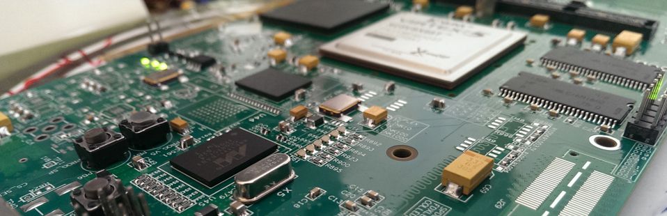
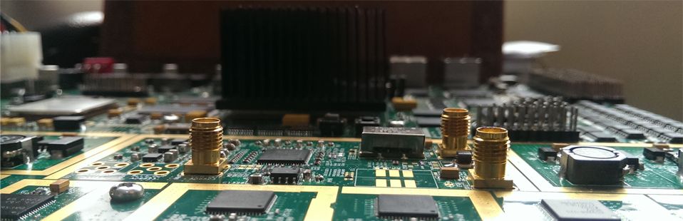
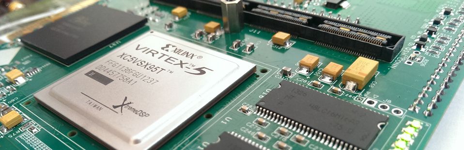
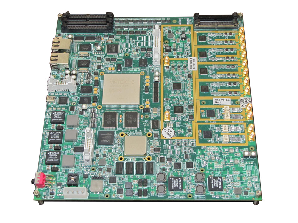
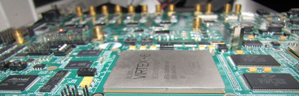
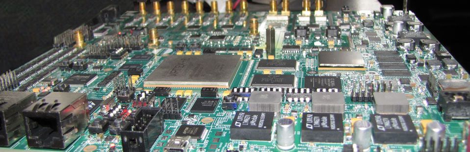
The NKS-V016-D processing board is a high performance industrial single card dedicated to high performance data acquisition and communications based on the Xilinx Virtex-6 XC6VSX315T FPGA family. The NKS-V016-D board enables designers to prototype high-performance digital transceivers. The board includes a DSP Processor (TMS320C6678) which incorporating the new and innovative C66x DSP core, this device can run at a core speed of up to 1.25 GHz. Additionally, four D/A channels 16-bit resolution at maximum rate of 1GSPS per channel and eight A/D channels 16-bit resolution at maximum rate of 250 MSPS per channel are available. The sample clock can be supplied from PLL clock distributor, externally through a coax connection or supplied by an internal clock source.


Features


ADC's:

  • 8 Channels, 16 bit, 250MSPS
  • Differential Analog Input with 650MHz Bandwidth
  • Analog Input Filter Options
  • SNR = 75 dBFS @ 20 MHz and 125 MSPS
  • SFDR > 80 dBc @ 20 MHz and 125 MSPS
  • ENOB = 12.4 Bits @ 20 MHz and 125 MSPS
  • Xtalk Isolation > 95dB
  • Low Power: 750 mW @ 125 MSPS
  • High Performance AC-Coupled Analog Input
  • 1.8 V Analog Supply Operation
  • 1.8 V CMOS or LVDS Output Supply
  • Flexible Analog Input Range: 1V p-p to 2V p-p

 DAC's:

  • 4 Channels, 16-Bit, 1GSPS Update Rate
  • Analog Output with 500MHz Bandwidth
  • Analog Output Filter Options
  • Phase Noise > 100dBc @ 1kHz and 1GSPS
  • Interleaved I/Q data for Dual-DAC Mode
  • 2x-32x Clock Multiplying PLL/VCO
  • 2x or 4x Interpolation Filters
  • High Performance AC-Coupled Analog Output with 2 Channel AC/DC Coupled Switching Capability

Clock's:

  • Flexible Synchronous PLL Clock Tree with Internal or External Clock
  • On board 200MHz Oscillator

Processor's:

  • Virtex-6 XC6VSX315T-2FFG1759I Xilinx Device
  • Digital Signal Processing (DSP)
  • TMS320C6678 TI Device
  • ARM Microcontroller AT91SAM7X256 Atmel Device
  • SP3XC3S200AN-4FTG256I for Power Sequence and DSP Separate Configuration

Memory's:

  • 4 Gb DDR3 Component Memory (Two [256 Mb x 8] Devices) for Virtex-6 FPGA
  • 8 Gb DDR3 Component Memory for DSP
  • 1 Mb I2C EEPROM for DSP local boot (remote boot possible)
  • 128 Mb NOR Flash for DSPSPI local boot
  • 144 Mb @ 167MHz SRAM Component Memory (Two [4Mb x 18] Devices)

Interface's:

  • Ethernet PHY 10/100/1000 Interface with RJ-45 Connector for FPGA and DSP
  • GPIO, EMIF, SRIO and PCIe Interface between FPGA and DSP
  • On-Board XDS100 type Emulation using High-speed USB 2.0 interface for DSP
  • RS232/RS485 UART for DSP
  • 8x Buffered TTL IN and 8x Buffered TTL OUT
  • 24x full-duplex, 2x half-duplex and1x Isolated RS485, 24x GPIO and 1x CAN BUS Serial Interfaces

Other's:

  • Multi-boot Configuration
  • Status and Debug LEDs
  • Power on/off Slide Switch
  • Physical Dimensions (L: 249.9 mm, W: 233.2 mm)
  • Operating temperature: -40°C to +85°C (Industrial)
  • 8V ~ 15V External Voltage Supply
  • Maximum Power Consumption in Full Load: 160W
  • Operation System Support: Windows & Linux


Block Diagram
niksoo
 
Application
  • RADAR/SONAR
  • Communications
  • Diversity radio systems
  • Multimode digital receivers (3G)
  • GSM, EDGE, W-CDMA, LTE
  • General-purpose software radios
  • Broadband data applications
  • I/Q demodulation systems
  • Fire Control and Defense Systems
  • Smart antenna systems


Documents
Download
NIKSOO Wave Processing Technology Engineering Corporation operates in the field of Biomedical, electronics and telecommunication, base-band and signal processing, installation and lunching, consulting and software production.
  btndownload


© copy right 2012 &all rights reseved by NIKSOO Wave Processing Technology Engineering Corporation